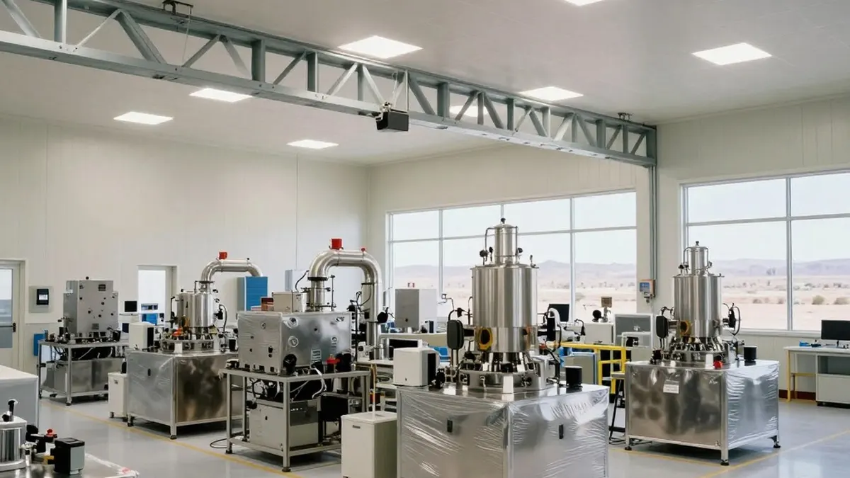
Intel announced on Wednesday that it has begun installing production tools at Fab 62, its new semiconductor facility in Arizona. The company said the plant is on track to be operational before the end of 2028, and it also gave updates on its Ohio manufacturing complex and on the use of High-NA EUV lithography in volume production.
In a statement, Naga Chandrasekaran, Intel Foundry's executive vice president and chief technology and operations officer, drew a distinction between products made in America and technologies that are "truly American-made." He said the difference lies in the research and development process that turns ideas into manufacturable technologies.
Fab 62 will be the sixth high-volume fab at Intel's Ocotillo campus in Arizona, a site that has been among the company's main production hubs for decades. The shell of the building was finished some time ago, so the start of tool installation shows the project has moved past construction. Intel has not said when high-volume output will start, how much wafer capacity the fab will have, how much capital the project needs, or which process nodes it will run.
The node question remains open. When Intel first announced Fab 52 and Fab 62, it said the pair would build its most advanced technologies, including Intel 20A and 18A. Fab 52 was later designated for Intel 18A, and Fab 62 has not been assigned. Under the process roadmap Intel disclosed earlier this year, the site could make chips on 18A, 18A-P and 14A. It could therefore add 18A capacity or serve as a home for 14A, though Intel has not confirmed either option.
On lithography, Intel was the first chipmaker to install a commercial High-NA EUV scanner, at its D1X fab near Hillsboro, Oregon. The company has since put the tool into high-volume manufacturing, using it to make select tiles for its Panther Lake processors and other chips. D1X is the site where Intel develops its most advanced logic processes and begins volume production of new processors. Intel has not explicitly confirmed it, but High-NA scanners appear for now to be producing the same circuits as Low-NA EUV machines, so they may not yet offer major advantages over existing equipment.
In Ohio, construction crews recently installed the first major structural truss at the first fab of the Ohio One complex in New Albany. Intel presents the project as part of its long-term plan to expand domestic production of chips on leading-edge processes. The company did not provide an updated construction schedule, a start date for operations, the process technology the fab will use, or its expected capacity, so it remains unclear when Ohio One will add to Intel's output.
Intel also pointed to investments elsewhere in the country. Oregon is its main research center for advanced logic and 3D interconnect technologies, while Arizona hosts advanced packaging R&D, assembly and testing. New Mexico is where Intel produces complex multi-chiplet processors using packaging methods ranging from EMIB to the newer EMIB-T and Foveros. The company has also recently broken ground on a photomask manufacturing facility in Santa Clara, California.
The source report argues these moves put Intel ahead of its rivals, noting that it is the only chipmaker in the United States developing and producing leading-edge chips entirely in the country. Samsung and TSMC currently lack leading-edge process R&D in America and do not run their own photomask shops there, and Samsung has abandoned a plan for an advanced packaging plant in Texas. Intel still relies on tools from Europe and materials from Japan.
Intel said its U.S. operations involve more than 4,500 suppliers across 49 states, with annual domestic spending above $29 billion. The company stressed that domestic semiconductor leadership requires not only wafer fabrication capacity but also research, process development, advanced packaging and a comprehensive supply chain.